清华大学 电子工程系/北京国家信息科学技术研究中心, 北京 100084
随着射频通信频谱资源的逐渐饱和,局域范围内高速通信亟需开辟一条新的赛道,而可见光通信得益于光的大带宽本质和通信范围有限而频谱免许可,是传统通信的理想补充之一。GaN基蓝绿光发光光源近十年来的快速发展,特别是性能优良的小尺寸高速光源microLED的发展,使其成为“万物互联”的物联网时代终末端通信的重要促进力量。文章分蓝绿光microLED和带有谐振腔的GaN基蓝绿光光源(含超辐射发光二极管和激光器)两个主要类别,回顾了蓝绿光高速光源的发展历程和最新进展,主要包括microLED结构与阵列、面发射腔增强光源、边发射腔增强光源三个方面。
光通信 氮化镓 高速 谐振腔 optical communication gallium nitride highspeed microLED microLED resonator
红外与激光工程
2022, 51(5): 20220270
清华大学 电子工程系/北京信息科学与技术国家研究中心, 北京 100084
超宽带光电子芯片是下一代无线通信、先进电子信息装备中光纤传输与信号处理的关键元器件, 芯片中光子、电子、电磁场之间的相互作用是决定芯片性能的核心因素。文章通过介绍超宽带光电探测器芯片、电光调制器芯片等方面的研究进展, 分享课题组在破解上述核心科学问题、提高芯片性能的关键技术方案。
光电子芯片 光探测器 电光调制器 optoelectronic devices photodetectors optical modulators
红外与激光工程
2021, 50(7): 20211052
Author Affiliations
Abstract
Beijing National Research Center for Information Science and Technology (BNRist), Department of Electronic Engineering, Tsinghua University, Beijing 100084, China
A novel thin-film lithium niobate (TFLN) electro-optic modulator is proposed and demonstrated. -silica hybrid waveguide is adopted to maintain low optical loss for an electrode spacing as narrow as 3 µm, resulting in a low half-wave-voltage length product of only 1.7 V·cm. Capacitively loaded traveling-wave electrodes are employed to reduce the microwave loss, while a quartz substrate is used in place of a silicon substrate to achieve velocity matching. The fabricated TFLN modulator with a 5-mm-long modulation region exhibits a half-wave voltage of 3.4 V and a merely less than 2 dB roll-off in an electro-optic response up to 67 GHz.
lithium niobate electro-optic modulator wideband half-wave voltage Chinese Optics Letters
2021, 19(6): 060016

Author Affiliations
Abstract
1 Beijing National Research Center for Information Science and Technology (BNRist), Department of Electronic Engineering, Tsinghua University, Beijing 100084, China
2 Tsinghua-Berkeley Shenzhen Institute (TBSI), Tsinghua University, Shenzhen 518055, China
3 Shenzhen International Graduate School, Tsinghua University, Shenzhen 518055, China
4 Institute of Electronics Engineering, Taiwan Tsing Hua University, Hsinchu 30013, Taiwan, China
5 e-mail: wanglai@tsinghua.edu.cn
6 e-mail: hyfu@sz.tsinghua.edu.cn
7 e-mail: mcwu@ee.nthu.edu.tw
The data rate of a visible light communication (VLC) system is basically determined by the electrical-to-optical (E-O) bandwidth of its light-emitting diode (LED) source. In order to break through the intrinsic limitation of the carrier recombination rate on E-O bandwidth in conventional c-plane LEDs based on InGaN quantum wells, a blue micro-LED with an active region of nano-structured InGaN wetting layer is designed, fabricated, and packaged to realize a high-speed VLC system. The E-O bandwidth of the micro-LED can reach up to 1.3 GHz. Based on this high-speed micro-LED, we demonstrated a data rate of 2 Gbps with a bit error rate (BER) of with simple on-off keying signal for a 3-m real-time VLC. In addition, a 4-Gbps VLC system using quadrature phase shift keying-orthogonal frequency-division multiplexing with a BER of is also achieved for the same scenario. Among all the point-to-point VLC systems based on a single-pixel LED, this work has the highest distance-bandwidth product of 3 GHz·m and the highest distance-rate product of 12 Gbps·m.
Photonics Research
2021, 9(5): 05000792
清华大学电子工程系,北京国家信息科学技术研究中心,北京 100084
目前,c面氮化镓(GaN)基发光二极管的制备技术已经十分成熟并取得了商业化成功,但仍面临极化电场导致的大电流密度下效率下降(Droop效应)和黄绿光波段效率低的问题。为消除极化电场的影响,人们开始关注半极性和非极性面GaN。其中,基于传统极性面衬底通过三维结构生长来获得半极性和非极性GaN的方法,由于其低成本和生长的灵活性,受到了广泛研究。本文首先总结了三种GaN三维结构的制备方法并分析其生长机理。接着,在此基础上介绍了不同晶面InGaN量子阱的外延生长和发光特性。最后,列举了GaN基三维结构在半极性面LED、颜色可调LED和无荧光粉白光发光二极管方面的应用。
氮化镓 发光二极管 三维结构 无荧光粉白光 效率下降 GaN lightemitting diode threedimensional structure phosphorfree white light efficiency droop
1 清华大学 电子工程系 北京信息科学与技术国家研究中心, 北京 100084
2 清华大学 柔性电子技术研究中心, 北京 10084
3 浙江清华柔性电子技术研究院 柔性智能光电子技术研究所, 浙江 嘉兴 314006
设计了一种适合集成的基于介质超表面的透射式光束偏转器, 可在1 550 nm附近的红外波段实现大角度偏转, 同时具有宽光谱、高效率的优势。根据广义斯涅尔定律设计并优化了光束偏转器的结构, 由横截面为梯形的非晶硅纳米柱周期性排列在石英玻璃衬底上构成, 相比于传统超表面采用多个纳米柱实现离散的相位梯度, 梯形纳米柱形成的连续相位梯度可以获得更好的偏转特性。利用时域有限差分算法对光束偏转器的效率、偏转角、宽光谱和入射角度依赖性等性能进行了仿真分析, 采用电子束光刻等工艺制备加工出上述器件并进行了测试。仿真结果表明: 偏转器在1 350~1 650 nm波段均具备良好的偏转特性, 平均透射率高于87%, 平均偏转率为81%; 器件在1 550 nm处实现了42.8°的大偏转角, 透射率为84%, 偏转率为80%, 且允许入射角度在-10°~5°变化。实验测试结果表明: 对于1 550 nm波长, 光束偏转角度在41°附近, 器件透射率约为76%, 约35%的入射光偏转到目标角度。上述方案为近红外超表面器件的设计提供了新的思路, 实现了效率、偏转角和适用波长的优化, 透射式光路更加适合集成, 应用潜力更大。
近红外 宽光谱、大偏转角 光束偏转器 介质超表面 梯形纳米柱 near-infrared broadband and large deflection angle beam deflector dielectric metasurface trapezoidal nanopillars
Author Affiliations
Abstract
1 Beijing National Research Center for Information Science and Technology (BNRist), Department of Electronic Engineering, Tsinghua University, Beijing 100084, China
2 Center for Flexible Electronics Technology, Tsinghua University, Beijing 100084, China
3 Flexible Intelligent Optoelectronic Device and Technology Center, Institute of Flexible Electronics Technology of THU, Jiaxing 314006, China
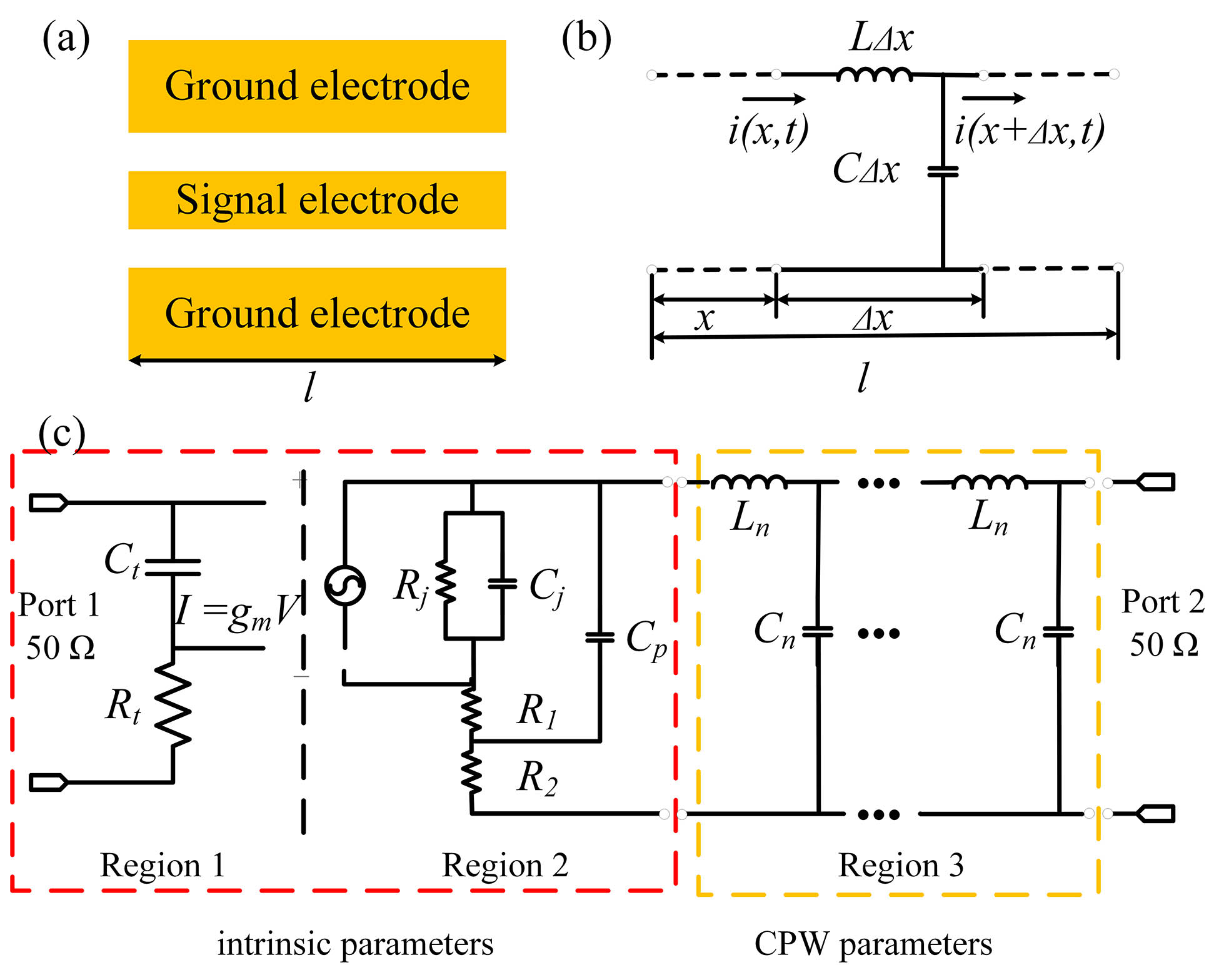
An equivalent circuit model including multi-section distributed parameters is proposed to analyze wideband photodiodes (PDs) with coplanar waveguide (CPW) electrodes. The model helps extract CPW parameters as well as intrinsic bandwidth parameters so that the influence of the CPW structure can be investigated, making it valuable for the design of high-performance PDs. PDs with an inductive 115 Ω impedance CPW are fabricated, and the 3 dB bandwidth is improved from 28 GHz to 37.5 GHz compared with PDs with a conventional 50 Ω impedance CPW.
photodiodes photodetector high-impedance coplanar waveguide Chinese Optics Letters
2020, 18(6): 061301

Author Affiliations
Abstract
1 Department of Electronic Engineering and Beijing National Research Center for Information Science and Technology, Tsinghua University, Beijing 100084, China
2 Beijing Engineering Research Center of Mixed Reality and Advanced Display, School of Optics and Photonics, Beijing Institute of Technology, Beijing 100081, China
3 State Key Laboratory for Mesoscopic Physics, Collaborative Innovation Center of Quantum Matter, and School of Physics, Peking University, Beijing 100871, China
Photon upconversion with transformation of low-energy photons to high-energy photons has been widely studied and especially applied in biomedicine for sensing, stimulation, and imaging. Conventional upconversion materials rely on nonlinear luminescence processes, suffering from long decay lifetime or high excitation power. Here, we present a microscale, optoelectronic infrared-to-visible upconversion device design that can be excited at low power (). By manipulating device geometry, illumination position, and temperature, the device luminescence decay lifetime can be tuned from tens to hundreds of nanoseconds. Based on carrier transportation and circuit dynamics, theoretical models are established to understand the transient behaviors. Compared with other mechanisms, the optoelectronic upconversion approach demonstrates the shortest luminescence lifetime with the lowest required excitation power, owing to its unique photon–electron conversion process. These features are expected to empower the device with essential capabilities for versatile applications as high-performance light emitters.
Photonics Research
2019, 7(10): 10001161


